1. Force sensing resistor gives a resistance value with respect to the force that is applied on it. Try
different loads (Pinching, squeezing with objects, etc.) and write down the resistance values.
(EXPLAIN with TABLE)
Figure 1: Table displaying force sensing resistor values
The more pressure present on the sensor, less resistance will be applied.
2. 7 Segment display:
a. Check the manual of 7 segment display. Pdf document’s page 5 (or in the document page 4)
circuit B is the one we have. Connect pin 3 or pin 14 to 5 V. Connect a 330 Ω resistor to pin
1. Other end of the resistor goes to ground. Which line lit up? Using package dimensions and
function for B (page 4 in pdf), explain the operation of the 7 segment display by lighting up
different segments. (EXPLAIN with VIDEO).
Figure 2: Video displaying 7 segment display.
b. Using resistors for each segment, make the display show 0 and 5. (EXPLAIN with PHOTOs)
Figure 3: Displaying a 0 with the 7 segment display.
Figure 4: Displaying a 5 with the 7 segment display.
3. Display driver (7447). This integrated circuit (IC) is designed to drive 7 segment display through
resistors. Check the data sheet. A, B, C, and D are binary inputs. Pins 9 through 15 are outputs that
go to the display. Pin 8 is ground and pin 16 is 5 V.
a. By connecting inputs either 0 V or 5 V, check the output voltages of the driver. Explain how
the inputs and outputs are related. Provide two different input combinations. (EXPLAIN
with PHOTOs and TRUTH TABLE)
Figure 5: Picture representation of circuit.
In the circuit, the display driver was used to light up the LED to show that voltage was being given because it could not be measured with the DMM.
Figure 6: Truth table for the 7447 display driver.
b. Connect the display driver to the 7 segment display. 330 Ω resistors need to be used between the display driver outputs and the display (a total of 7 resistors). Verify your question 3a outputs with those input combinations. (EXPLAIN with VIDEO)
Figure 7: Video showing how the 7447 display driver works.
4. 555 Timer:
a. Construct the circuit in Fig. 14 of the 555 timer data sheet. VCC = 5V. No RL (no connection to
pin 3). RA = 150 kΩ, RB = 300 kΩ, and C = 1 µF (smaller sized capacitor). 0.01 µF capacitor is
somewhat larger in size. Observe your output voltage at pin 3 by oscilloscope. (Breadboard
and Oscilloscope PHOTOs)
Figure 8: Picture representation of circuit.
Figure 9: Output voltage of pin 3 of circuit in figure 8.
b. Does your frequency and duty cycle match with the theoretical value? Explain your work.
Based on the calculations we acquired, the frequency and duty cycle are accurate. We found this by using the equations below, which are dependent on Ra, Rb and the capacitor.
Figure 10: Equations used to calculate frequency and duty cycle.
c. Connect the force sensing resistor in series with RA. How can you make the circuit give an
output? Can the frequency of the output be modified with the force sensing resistor?
(Explain with VIDEO)
Figure 11: Video showing how the force sensing resistor works.
5. Binary coded decimal (BCD) counter (74192). This circuit generates a 4-bit counter. With every clock change, output increases; 0000, 0001, 0010, …, 0111, 1000, 1001. But after 1001 (which is decimal 9), it goes back to 0000. That way, in decimal, it counts from 0 to 9. Outputs of 74192 are labelled as QA (Least significant bit), QB, QC, and QD (Most significant bit) in the data sheet (decimal counter, 74192). Use the following connections: 5 V: pins 4, 11, 16. 0 V (ground): pins 8, 14. 10 µF capacitor between 5 V and ground.
a. Connect your 555 timer output to pin 5 of 74192. Observe the input and each output on the oscilloscope. (EXPLAIN with VIDEO and TRUTH TABLE)
Figure 12: Video explaining how the 555 timer works in combination with the 74192.
Figure 12:Data Table
6. 7486 (XOR gate). Pin diagram of the circuit is given in the logic gates pin diagram pdf file. Ground pin is 7. Pin 14 will be connected to 5 V. There are 4 XOR gates. Pins are numbered. Connect a 330 Ω resistor at the output of one of the XOR gates.
a. Put an LED in series to the resistor. Negative end of the LED (shorter wire) should be connected to the ground. By choosing different input combinations (DC 0V and DC 5 V), prove XOR operation through LED. (EXPLAIN with VIDEO)
Figure 13: Video showing the XOR operation with the LED.
b. Connect XOR’s inputs to the BCD counters C and D outputs. Explain your observation. (EXPLAIN with VIDEO)
Figure 14: Video explaining the XOR outputs vs inputs.
c. For 6b, draw the following signals together: 555 timer (clock), A, B, C, and D outputs of 74192, and the XOR output. (EXPLAIN with VIDEO)
Figure 15: Signals for 555 timer, A,B,C and D outputs of 74192 and XOR output.
Figure 16: Video explaining output signals.
7. Connect the entire circuit: Force sensing resistor triggers the 555 timer. 555 timer’s output is used as clock for the counter. Counter is then connected to the driver (Counter’s A, B, C, D to driver’s A, B, C, D). Driver is connected to the display through resistors. XOR gate is connected to the counter’s C and D inputs as well and an LED with a resistor is connected to the XOR output. Draw the circuit schematic. (VIDEO and PHOTO)
Figure 17: Video showing entire circuit functioning.
Figure 18: Picture of entire circuit.
8. Using other logic gates provided (AND and OR), come up with a different LED lighting scheme. (EXPLAIN with VIDEO)
Figure 19: Video showing different lighting scheme.
We didn't have access to a different logic gate so instead we just used the XOR gate but with different input values.
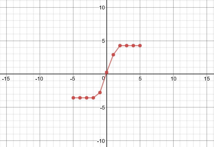
1. You will use the OPAMP in “open-loop” configuration in this part, where input signals will be applied directly to the pins 2 and 3.
a. Apply 0 V to the inverting input. Sweep the non-inverting input (Vin) from -5 V to 5 V with 1 V steps. Take more steps around 0 V (both positive and negative). Create a table for Vin and Vout. Plot the data (Vout vs Vin). Discuss your results. What would be the ideal plot?
Figure 1: Table displaying Vin vs. Vout for non-inverting amplifier.
The graph shows the change in values for Vout.
Due to the amplifier being non inverting, the Vout was the same sign as Vin. The output was also amplified as shown until reaching a certain Vin where a max Vout is reached and it becomes constant (-4.2 and 4.52). The ideal plot would be 0 output at 0 and then the exact measurement for gain.
b. Apply 0 V to the non-inverting input. Sweep the inverting input (Vin) from -5 V to 5 V with 1 V steps. Take more steps around 0 V (both positive and negative). Create a table for Vin and Vout. Plot the data (Vout vs Vin). Discuss your results. What would be the ideal plot?
Figure 2: Table displaying Vin vs. Vout for inverting amplifier.
The graph shows the change in values for Vout.
As expected, due to the amplifier being inverting the Vout values were the opposite sign as Vin. The output was also amplified just as the non-inverting was, once it reached a max Vout, the amplification became constant at (4.52 and -4.2). The ideal plot would be 0 output at 0 and then the exact measurement for gain.
2. Create a non-inverting amplifier. (R2 = 2 kΩ, R1 = 1 kΩ). Sweep Vin from -5 V to 5 V with 1 V steps. Create a table for Vin and Vout. Plot the measured and calculated data together.
Figure 3: Table displaying Vin vs. Vout for the non-inverting amplifier.
Graph Vout for the non-inverting amplifier
For the non inverting amplifier the gain was 3. This can be seen when Vin is 1V but then Vout reaches its max at (4.27 or -3.56).
3. Create an inverting amplifier. (Rf = 2 kΩ, Rin = 1 kΩ). Sweep Vin from -5 V to 5 V with 1 V steps. Create
a table for Vin and Vout. Plot the measured and calculated data together.
Figure 4: Table displaying Vin vs. Vout for inverting amplifier.
Graph for Vout.
For the inverting amplifier the gain was 2 as shown when Vin is 1V. After this, Vout reaches its max at (4.21 or -3.5).
4. Explain how an OPAMP works. How come is the gain of the OPAMP in the open loop configuration
too high but inverting/non-inverting amplifier configurations provide such a small gain?
An OPAMP takes an input signal and amplifies it and can also invert the polarity of the signal if the OPAMP is set in inverting configuration. However, the output signal can not be higher than the values put into V+ and V-. When the OPAMP is in open loop configuration there are no resistors to implement a low enough gain and therefore the gain is very high and often reaches higher than V+ or V- very easily.
TEMPERATURE CONTROLLED LED SYSTEM
1. Connect your DC power supply to pin 2 and ground pin 5. Set your power supply to 0V. Switch
your multimeter to measure the resistance mode; use your multimeter to measure the
resistance between pin 4 and pin 1. Do the same measurement between pin 3 and pin 1. Explain
your findings (EXPLAIN)
Between pin 4 and pin 1 we measured a resistance of 2 Ohms. And the resistance between pin 3 and 1 gave us an overload because pin 3 wasn't connected to the circuit due to Vin being less than Vthreshold.
2. Now sweep your DC power supply from 0V to 8V and back to 0V. What do you observe at the
multimeter (resistance measurements similar to #1)? Did you hear a clicking sound? How many
times? What is the “threshold voltage values” that cause the “switching?” (EXPLAIN with a
VIDEO)
Figure 5: Video explaining the circuit.
3. How does the relay work? Apply a separate DC voltage of 5 V to pin 1. Check the voltage value
of pin 3 and pin 4 (each with respect to ground) while switching the relay (EXPLAIN with a
VIDEO).
Figure 6: Video explaining how a relay works.
LED RELAY
1. Connect positive end of the LED diode to the pin 3 of the relay and negative end to a 100 ohm
resistor. Ground the other end of the resistor. Negative end of the diode will be the shorter
wire.
2. Apply 3 V to pin 1
3. Turn LED on/off by switching the relay. Explain your results in the video. Draw the circuit
schematic (VIDEO)
Figure 7: Picture representation of the circuit.
Figure 8: Video showing how the relay circuit works.
OPERATIONAL AMPLIFIER
1. Connect the power supplies to the op-amp (+10V and 0V). Show the operation of LM 124
operational amplifier in DC mode with a non-inverting amplifier configuration. Choose any
opamp in the IC. Method: Use several R1 and R2 configurations and change your input voltage
(voltages between 0 and 10V) and record your output voltage. (EXPLAIN with a TABLE)
Figure 1: Picture displaying function check on oscilloscope
The function check was obtained on the oscilloscope by connecting the probe to the 5v output on the device and the ground clip to the ground.
2. Perform manual probe compensation (Oscilloscope manual page 8) (Photo of overcompensation and proper compensation).
Figure 2: Proper compensation
Our probe was already calibrated when we got it so it did not require any compensation.
3. What does probe attenuation (1x vs 10x) do (Oscilloscope manual page 9)?
Probe attenuation controls the bandwidth of the oscilloscope. 10x uses full bandwidth while 1x is limited to 7MHz. While in 10x the amplitude of the signal will be reduced to a 10th of 1.
4. How do vertical and horizontal controls work? Why would you need it (Oscilloscope manual pages 34-35)?
The vertical controls the vertical axis(voltage) and the horizontal controls the horizontal axis(time).The controls work by translating the wave either vertically or horizontally, vertically for amplitude while horizontally is for frequency. You would need this to be able to see more or less of the wave.
5. Generate a 1 kHz, 0.5 Vpp around a DC 1 V from the function generator (use the output connector). DO NOT USE oscilloscope probes for the function generator. There is a separate BNC cable for the function generator.
a) Connect this to the oscilloscope and verify the input signal using the horizontal and
vertical readings (photo).
Figure 3: The picture above shows the oscilloscope at 1Khz and 0.5Vpp.
b) Figure out how to measure the signal properties using menu buttons on the scope.
Figure 4: Video shows how to measure the signal properties using menu buttons.
6. Connect function generator and oscilloscope probes switched (red to black, black to red). What happens? Why?
No signal is shown because when reversing the connection the output of the oscilloscope is grounded and completely negated.
7. After calibrating the second probe, implement the voltage divider current below. Measure the following voltages using the Oscilloscope and comment on your results:
Figure 5: picture depiction of the circuit being measured
a. Va and Vb at the same time (Photo)
Figure 6: Picture of the waves from the circuit above
b. Voltage across R4
The voltage across R4 is equal to the voltage of every other resistor in the same circuit.The value we got for Vpp was 0.75V.
8. For the same circuit above, measure Va and Vb using the handheld DMM both in AC and DC
mode. What are your findings? Explain.
In the table below we took note on the measurements that were acquired using the circuit presented on problem seven. We used handheld DMM, and we measured in both AC and DC. We found out that the voltage for Vb is exactly double the measure of Va.
Figure 7: Table of voltages obtained from the circuit
9. For the circuit below
a. Calculate R so given voltage values are satisfied. Explain your work (video)
Figure 8: Video explaining the calculations for R
b. Construct the circuit and measure the values with the DMM and oscilloscope (video).
Hint: 1kΩ cannot be probed directly by the scope. But R6 and R7 are in series and it does
not matter which one is connected to the function generator.
Figure 9: Video of voltages being measured.
Figure 10: Picture depiction of circuit in videos.
10. Operational amplifier basics: Construct the following circuits using the pin diagram of the
opamp. The half circle on top of the pin diagram corresponds to the notch on the integrated
circuit (IC). Explanations of the pin numbers are below:
Figure 11: Picture depiction of amplifier and pin diagram.
a. Inverting amplifier: Rin = 1kΩ, Rf = 5kΩ (do not forget -10 V and +10 V). Apply 1 Vpp @ 1kHz.
Observe input and output at the same time. What happens if you slowly increase the input
voltage up to 5 V? Explain your findings. (Video)
Figure 12: Video displaying inverting amplifier circuit
b. Non-inverting amplifier: R1 = 1kΩ, R2 = 5kΩ (do not forget -10 V and +10 V). Apply 1 Vpp @ 1kHz. Observe input and output at the same time. What happens if you slowly increase the input voltage up to 5 V? Explain your findings. (Video)
Figure 13: Video displaying non-inverting amplifier circuit.


 Figure 12:Data Table